
EUV Lithography: The Race To Nano. Process Nodes ReDefined.
- Borrow2Share

- Apr 13, 2024
- 3 min read
EUV Lithography: The Smaller The Light WaveLength, The Smaller The Feature Sizes.
"If we heat tin to an extremely high temperature, up to 400,000 degrees Celsius, then the atoms fall apart into free electrons and positively charged ions of differing charges. Furthermore, many of these ions are in an excited state: One or more of the orbiting electrons has an extra portion of energy. These electrons circle in an orbit that is further from the atomic nucleus than the closest orbit. When they return to an orbit closer to the nucleus, that additional energy is released in the form of EUV radiation," Versolato explains.
"In a tin ion, a single electron can have such an extra energy packet, but it is also possible that several electrons simultaneously have one. They orbit in the first, second third or even the fourth shell around the atomic nucleus. However, the probability of an electron reaching a higher excited state becomes increasingly smaller with each step upward. It was therefore generally assumed that electrons in the first excited state mainly emitted the EUV light in tin plasma."
By comparing their lab experiments with the calculations from Los Alamos, the researchers discovered that it is not just electrons that return from the first excited energy state which emit light at 13.5 nanometers. Electrons in higher shells also contributed to this, because the energy difference between successive excited states is the same.
"This means that each [and every] electron that returns to a lower energy state contributes to the emission of 13.5 nanometer light. That property makes tin plasma unique and exceptionally suitable as an EUV source," says Versolato.
On The History of EUV Lithography. A Very Good Summary of Events.
https://www.bloomberg.com/news/videos/2024-04-11/how-america-dropped-the-ball-on-key-chip-technology
__________________________________________________________________________
Semiconductor Chips Manufacturing. "Process Node" Generations. The Definition Changes.
In Semiconductor Chips Manufacturing, The Manufacturing "Process Node" Used To Be Defined By (Referred To) The Transistors' Their Gate Length In The Manufacturing Process. The Transistor's Gate Length Was The Minimum Feature Size And So Characterized Each Manufacturing Technology Generation As The Gate Length Got Smaller Each Time.
But Scaling Down The Transistor's Gate Length Reached It's Limit As Other Transistor Features Continue To Shrink Further. And The Transistor Form Also Changed From Planar FETs To 3D FinFETs. So Now The "Process Node" Follows the ITRS Definition.
International Technology Roadmap for Semiconductors.
ITRS Defines the "Process Node" as The Smallest Half-Pitch of Contacted Metal1 Layer Lines Allowed In The Fabrication Process. I Believe Metal1 Layer Lines Make Direct Connections To The Transistors' Drains/Sources.
"The Smallest Half-Pitch Is A Common Metric Used To Describe and Differentiate The Technology Generations Used in fabricating integrated circuits."
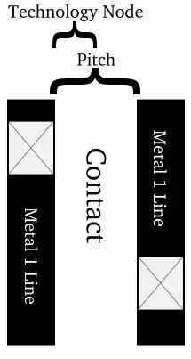
There Are Metal2 Layer Lines Providing Power and Ground. And Metal3 Layer, Metal4 Layer, And Etc Layers. The Metal Layers Serve As The Interconnects For All The Billions Of Transistors. How Else Would You Connect Up All The Transistors? With Power, Ground, And Carrying The Signals...
-----------------------------------
" Roughly for the first 35 years of the semiconductor history, since the first mass production of MOSFET in the 1960s to the late 1990s, the Process Node more or less referred to the Transistor's Gate Length (Lg) which was also considered the "Minimum Feature Size".
For example, Intel's 0.5 µm process had Lg = 0.5 µm. This lasted until the 0.25 µm process in 1997 at which point Intel started introducing more aggressive Gate Length Scaling.
In their 0.25 µm process it had Lg = 0.20 µm and likewise, in their 0.18 µm process had Lg = 0.13 µm (a node ahead). At those nodes the "Process Node" was effectively larger than the Gate Length. "
" At the 45 nm process, Intel reached a Gate Length of 25 nm on a traditional planar transistor. At that node the Gate Length Scaling effectively stalled; any further scaling to the gate length would produce less desirable results.
Following the 32 nm process node, while other aspects of the transistor shrunk, the Gate Length was actually increased.
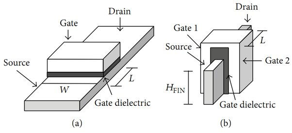
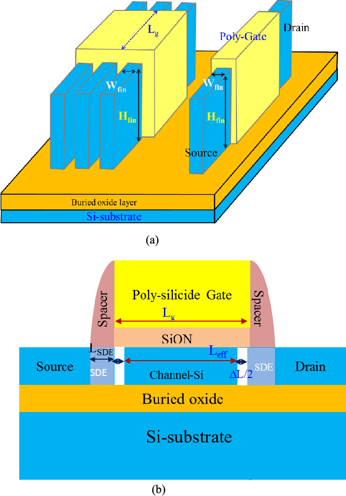
With the introduction of FinFET by Intel in their 22 nm process, the transistor density continued to increase all while the Gate Length remained more or less a constant. This is due to the properties of FinFET; for example the effective channel length is a function of the new fins (Leff = 2 * Hfin + Wfin).
Due to how the Transistor changed dramatically from how it used to be, the current Process Node naming scheme lost meaning. "
"The ITRS traditionally defined the Process Node as the smallest half-pitch of contacted metal1 layer lines allowed in the fabrication process. It is a common metric used to describe and differentiate the technologies used in fabricating integrated circuits."
So now, the Process Node defines the Smallest Half-Pitch of Contacted Metal1 Layer Lines allowed in the fabrication process. "


Comments